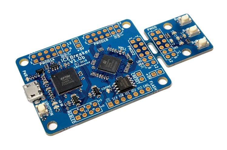
iCEBreaker
- iCE40UP5K in QFN48 (SG48) package
- iCE40 UltraPlus 5K
- 5280 Logic Cells (4-LUT + Carry + FF)
- 128 KBit Dual-Port Block RAM
- 1 MBit (128 KB) Single-Port RAM
- PLL, Two SPI and two I2C hard IPs
- Two internal oscillators (10 kHz and 48 MHz)
- 8 DSPs (16x16 multiply + 32 bit accumulate)
- 3x 24mA drive and 3x hard PWM IP
- QSPI-DDR-capable flash 128 MBit (16 MB)
- We selected to use the Winbond W25Q128JVSIM
- We want to enable projects that access the flash and we want to provide the highest flash access speed possible.
- FT2232H interface (microUSB plug)
- programming compatible with iCEstick and HX8K board
- works with Diamond Programmer and iceprog
- serial port compatible with iCEstick and HX8K breakout board
- 12 MHz XTAL oscillator (shared with FPGA)
- Solder jumpers to offer direct SRAM programming (like on HX8K breakout board)
- programming compatible with iCEstick and HX8K board
- 39 I/O capable pins:
- 4 pins for config (SDI, SDO, SCK, CSB)
- Either loading config from on board FLASH chip or provided through the FTDI chip with direct SRAM config.
- 2 extra GPIO pins for QSPI
- Together with the config pins, allows storage of additional data in the FLASH chip, and high speed QSPI DDR access. For example picosoc firmware.
- 3 PINs for RGB LED (pin header)
- 2 LEDs (one on output-only PLL pin)
- 1 Clock pin (on PLL GBIN)
- 1 UART Rx Pin via FTDI
- 1 UART Tx Pin via FTDI
- 1 Push Button
- 16 PINs on dual PMOD
- 8 PINs on single PMOD / snap-off section
- 4 pins for config (SDI, SDO, SCK, CSB)
- Support for FTDI Async FIFO mode
- We want to support FTDI Async mode via some (unpopulated by default) zero ohm resistors
- This shares 8 GPIOs with the single PMOD / snap-off section
- This would also enable use of full list of RS232 signals
- BDATA[0] – Tx on FTDI / Rx on FPGA (always connected, no zohm resistor required)
- BDATA[1] – Rx on FTDI / Tx on FPGA (always connected, no zohm resistor required)
- BDATA[7:2] – Shared with snap-off section (via zohm resistor footprint)
- RX Full – Shared with snap-off section (via zohm resistor footprint)
- TX Empty – Shared with snap-off section (via zohm resistor footprint)
- Read – Shared with LED 1 (via zohm resistor footprint, LED used as RX indicator)
- Write – Shared with LED 2 (via zohm resistor footprint, LED used as TX indicator)
- WakeUp – Shared with Push Button (via zohm resistor footprint)
- This configuration uses the following pins when the jumpers ore reconfigured:
- The two on board red and green LED pins
- The on board user button pin
- snap off section single PMOD pins
- Snap-off section (convertible to PMOD host / PMOD device)
- 5 LEDs in similar arrangement to iCEstick
- 3 Push Buttons
- Other stuff
- Status LEDs for Power and CDONE
- Header with supply rails: 5V, 3V3, 1V2, GND
- Debug header for all 6 QSPI pins
- Test points for UART Rx / Tx signals
- Jumpers or zohm resistors on all rails for measuring currents
- Four 3mm mounting holes on the main section and two more on the snap-off section
- The two LEDs on the main section should be wired “active low” so they work well as indicator LEDs for FIFO read/write.
- The five LEDs on the snap-off section should be wired “active high”
- A zohm resistor for Bank 2 supply so that the IO voltage can be changed. Use Bank 2 for one of the ports on the double PMOD.
- There should be auxilary 5V pin headers available for the PMODs. Some PMOD need either higher voltage or need to regulate their own voltage from 5V.
- Unpopulated parts shipped with the board
- 3x Host PMOD (2x for dual PMOD port, 1x for snap-off section)
- 1x Device PMOD (for other side of snap-off section)
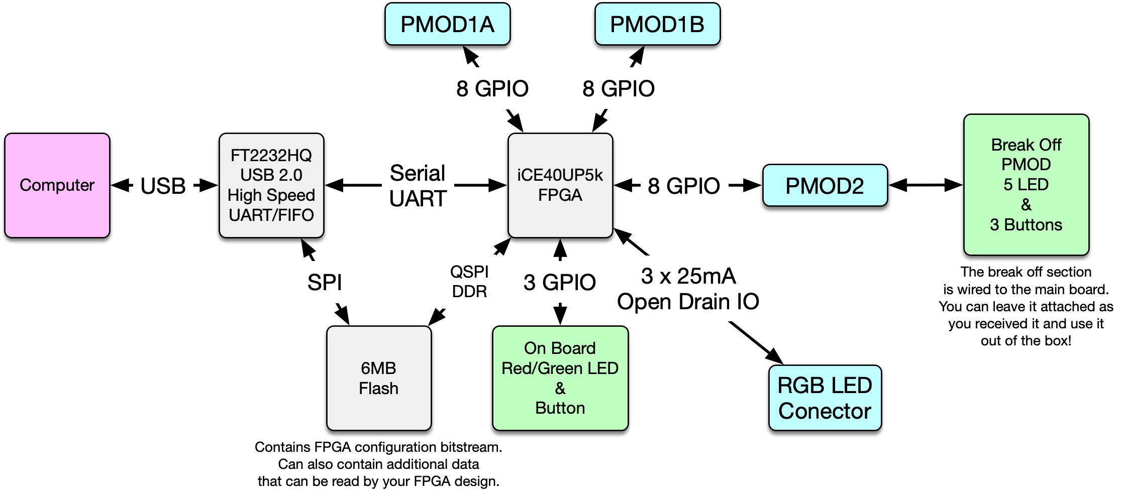 iCEBreaker block diagram
 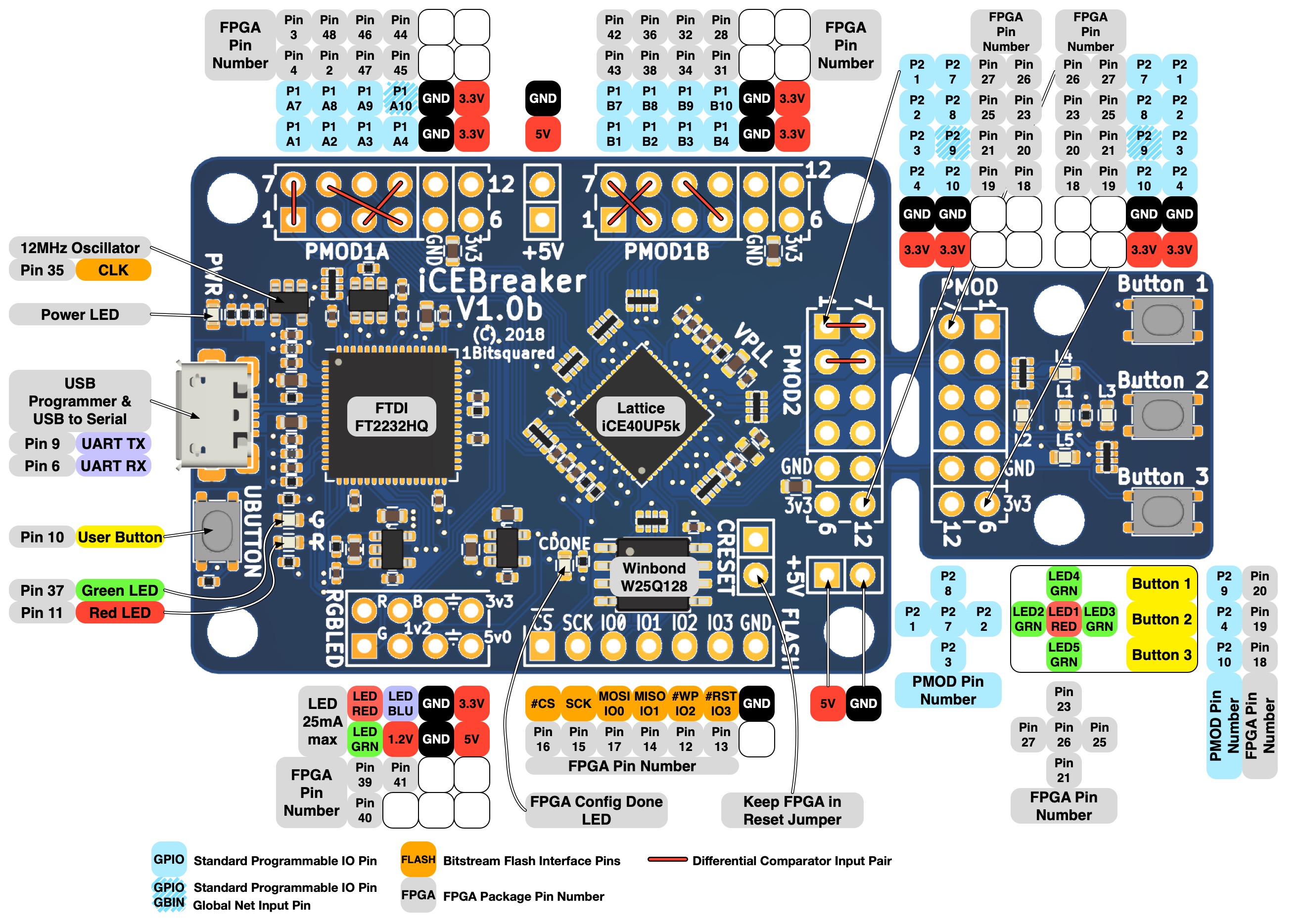 iCEBreaker V1.0b pinout legend
 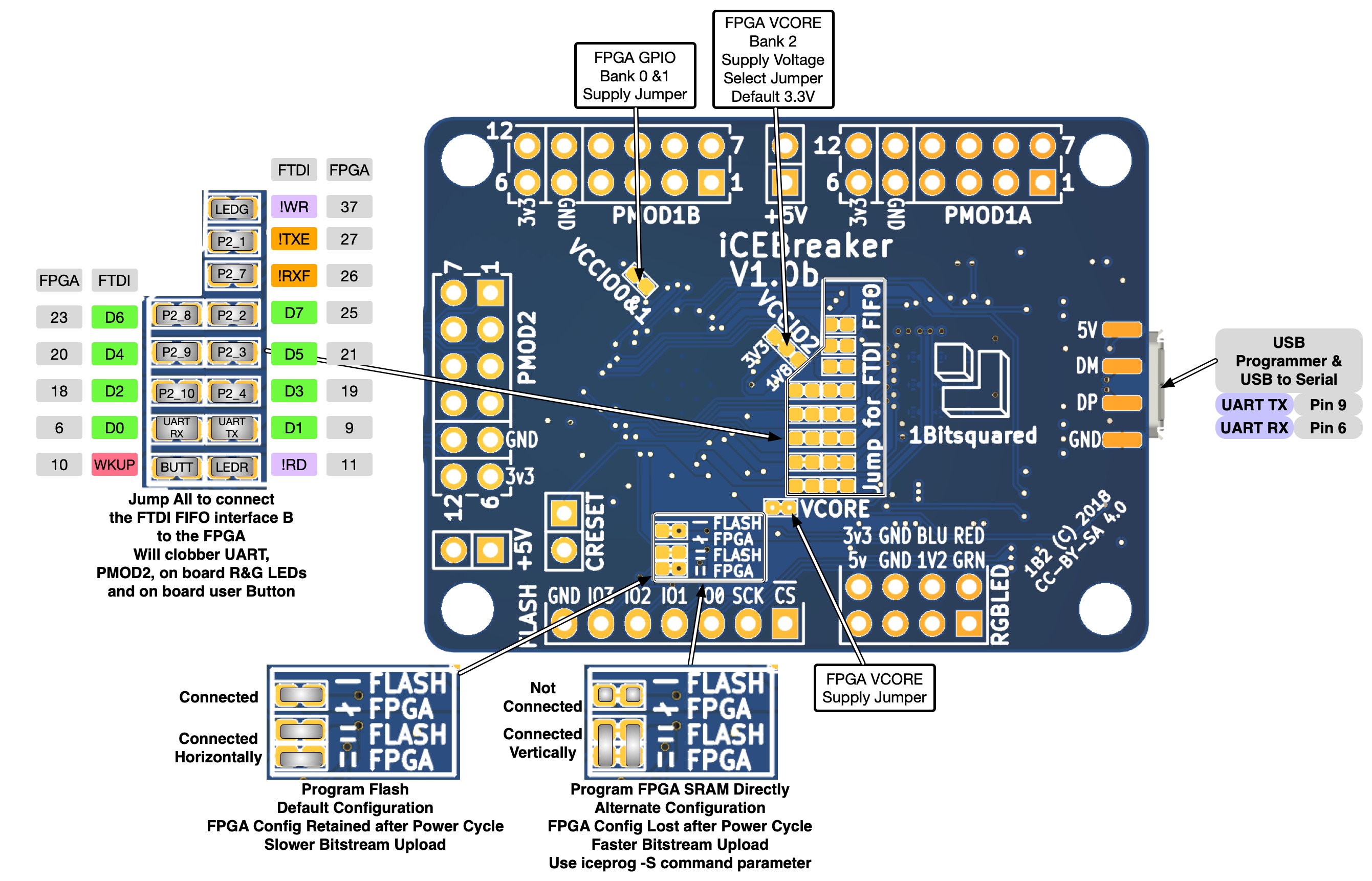 iCEBreaker V1.0b jumper legend